General Description
Microwave filters are used to pass or reject certain frequencies of a microwave signal. It is an essential component of many electronic systems and is used to separate signals that are close in frequency, attenuate unwanted signals, and improve overall system performance.
Filters are passive electronic components essential to communication systems. They can be found in a large variety of domains such as spatial, telecommunications, or defense.
When designing a new filter, the first step is to start by carefully determining the frequency range used in the system, and the frequencies that need to be cut off and therefore choosing the right type of filter. There we present you this general discussion around RF and microwave filters.
Filter types
Low Pass Filters
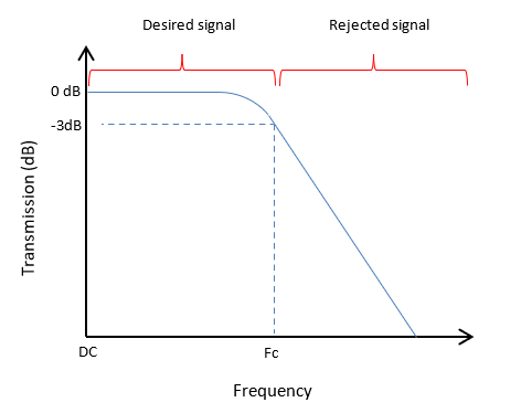
A low-pass filter is a type of electronic filter that allows low-frequency signals to pass through while attenuating high-frequency signals. It is a common filter used in electronic circuits to remove high-frequency noise or unwanted signals and to allow only the desired low-frequency signals to pass through.
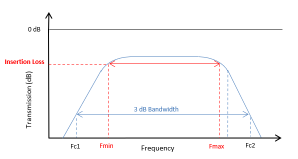
Indeed, a low pass filter lets the signal from direct current (DC) to a predefined cut off frequency (Fc) pass (defined most of the time @ -3 dB). All the frequencies above Fc are attenuated.
High Pass Filters
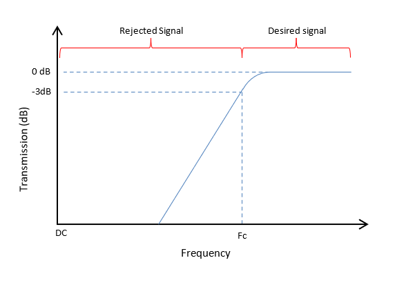
A high-pass filter is a type of electronic filter that allows high-frequency signals to pass through while attenuating low-frequency signals. It is the opposite of a low-pass filter, as it lets frequencies above the frequency cut off pass through while cutting off frequencies bellow Fc
Band Pass Filters
A bandpass filter selects a frequency range known as the passband. This selected bandwidth is defined by a low and a high frequency cut off. The signal outside this frequency range is attenuated.
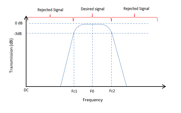
Bandpass filters are used in a wide range of applications, including radio communication systems, radar systems, and wireless networking. In radio communication systems, for example, bandpass filters are used to isolate the desired frequency range of a signal from other signals and noise that may be present in the environment.
Bandstop (Notch) Filters
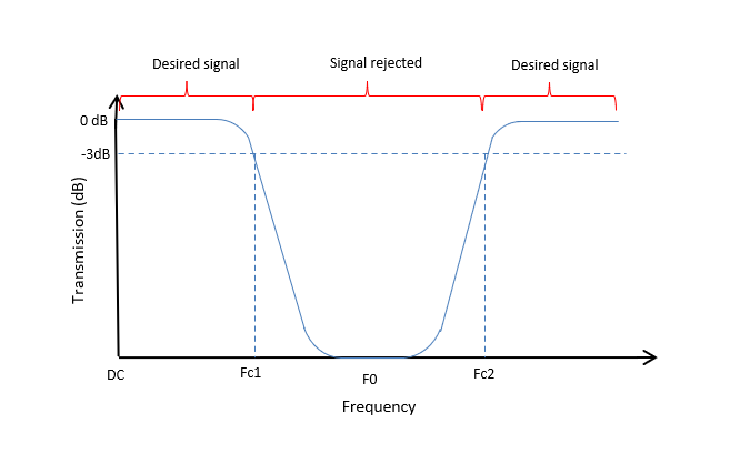
A bandstop filter, also known as a notch filter, is a type of electronic filter that attenuates a specific frequency range, known as the stopband, while allowing frequencies outside of this range to pass through. This type of filter is commonly used in electronic systems to suppress unwanted signals or noise within a specific frequency range.
The stopband of a bandstop filter is typically specified by the lower and upper cutoff frequencies (called Fc1 and Fc2 on the figure bellow), which define the range of frequencies that are attenuated by the filter. The width of the stopband is called the bandwidth and is defined as the difference between the upper and lower cutoff frequencies.
Bandstop filters are used in a wide range of applications, radio communication systems, and instrumentation. In radio communication systems, bandstop filters are used to suppress specific frequencies that may interfere with the desired signal.
Attributes and Specification Definition
Cut Off Frequency
The cut off frequency defines when the signal is attenuated by – 3dB which means that half the signal is transmitted and half is attenuated. It defines what is often called the 3dB bandwidth.
Insertion Loss
Insertion loss defines the amount of power loss within the frequency bandwidth of the signal, I.E. the difference of power between the input and the output. When designing a filter, we often look at minimizing this parameter as much as possible in order to limit data losses, and to improve the overall performance of the system. It often defines the usable bandpass of the filter.
Four kinds of losses can be distinguished:
- Dielectric loss : phenomenon linked to the dielectric properties of the material used.
- Conductor loss : linked to the resistivity of the material used to transport the signal.
- Mismatch loss : represents the amount of power loss due to defaults of impedance matching between the filter and its environments.
- Radiation losses : amount of rf power that leaks out of the product.
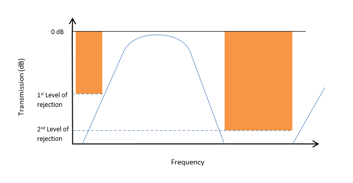
Attenuation/Rejection
Rejection is the level of power attenuation outside the bandwidth of the filter. Depending on the application and on the level of noise acceptable in the system, the rejections can be more or less strong.
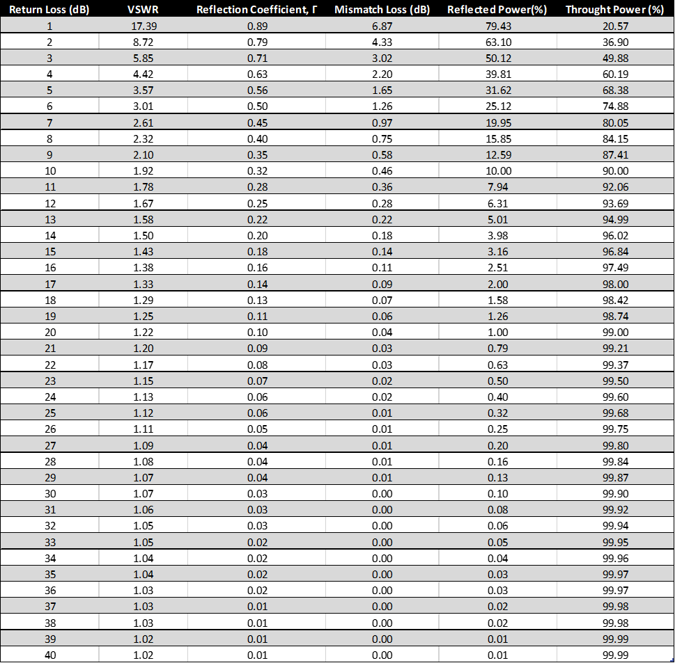
VsWR / Return Loss
The VSWR (Voltage Standing Wave Ratio) is a value used to quantify the level of impedance mismatch between a filter an its environment. The worst the mismatch is, the higher the VSWR will be. It allows to quantify the amount of power lost in reflection on the measured port.
For high power application, a bad matching can lead to strong impact on the device and the system such as high temperature, leading to connector or circuit failure.
The VSWR specification is, most of the time, defined on the same frequency bandwidth as the insertion loss. Indeed, on the rejected bandwidth the VSWR is high preventing the signal from going through the filter.
It is, however, possible to design absortive filters, which have the singularity of having a low VSWR even on the rejected frequency bands. This kind of filter is rare and limited to specific applications.
Group delay
Group delay quantifies the phase linearity seen by the signal when passing through the filter.
Power handling
The main limitation in terms of power handling the technology used for the filter. Indeed, it is mainly linked to the insertion loss as it is proportional to the amount of power that needs to be dissipated as heat. In order to maximize the heat dissipation, heat sinks or forced ventilation can be used.
Peak power handling leads to 2 distinct problematics:
- Equivalence with CW power handling as it can be approximated to Peq_cw=Ppeak x Duty Cycle, which lead similar issues as in the CW power handling paragraph.
- Peak power value it self that need to be consider as it can lead to electrical shorting if the distances between the high power signal and the ground are not properly taken into account.
Topologies
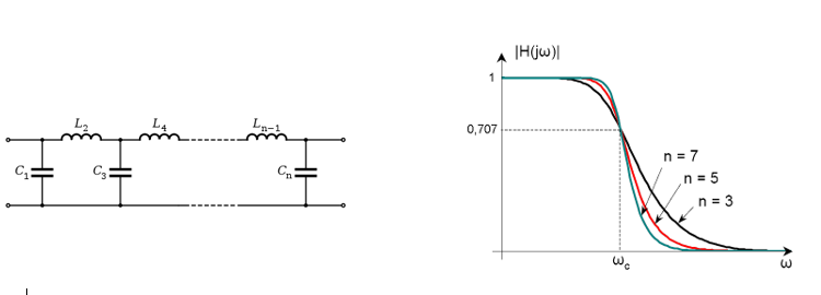
In order to design a filter, the most common way is to start with the synthesis of an ideal low pass filter and then to transpose it to another filter type (high pass, band pass, etc.). To do so, we use transfer functions, allowing the designer to define the topology of the filter and to compute the coefficient value needed to match the desired behavior. Each topology has its own distinctive characteristics.
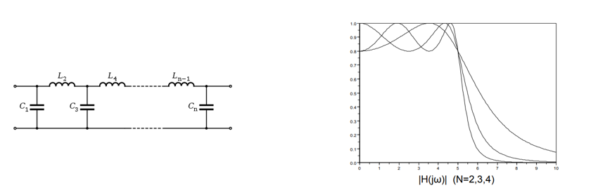
Butterworth
Butterworth filters are pretty standard as they are easy to design. The main advantage of this topologies is it constant gain within the bandwidth. The level of rejection steepness is dependent on the filter order, i.e. the number of resonant components (capacitors and inductors). Indeed, the higher the order is, the steeper the rejection is.
Chebyshev
Chebyshev topology gives selective filters but it leads to ripple either within the bandwidth (type 1) or within the rejected band (type2)
- Type 1
Unlike Butterworth, Chebyshev topology allows ripple within the bandwidth, leading to a steeper rejection. By increasing the order of the filter, we can get a steeper rejection but with a higher ripple.
- Type 2
Also called inverse Chebyshev, this topology slightly diverges from type 1. The response within the bandwidth is very flat, the ripple appears with the rejected band. One feature of this topology is the alternation between simple resonant elements with LC circuits (series or parallel). Chebyshev type 2 is least often used because it led to component values hard to reach and need a strong precision of the LC circuits.
Bessel
Bessel topology offers the best group delay, which means that all the frequencies within the bandwidth of the filter are transmitted with the same delay. However, the downside is that the rejection stepness is low (lower that with Butterworth), and raises very slowly as the filter order increases.
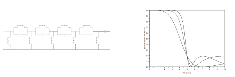
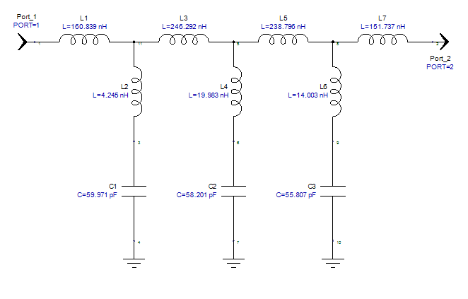
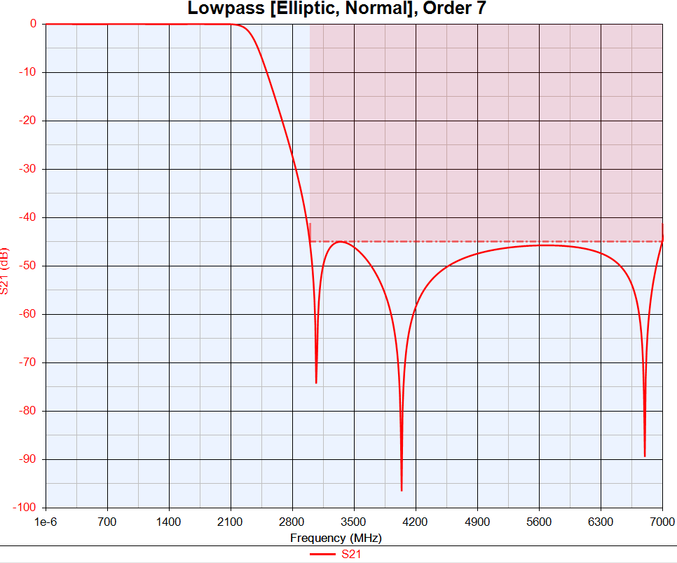
Elliptic (Cauer)
Elliptic filters (also called Cauer filters), allows a ripple on the whole frequency range. It leads to a very strong steepness of rejection, and therefore these filters are the most selective kind. As Chebyshev type 2 topology, it is made of LC circuits and simple capacitances and inductances. They can be quite hard to implement but give very good results.
The main downside of Elliptic filter is that the rejection does not increases past a certain frequency as it will stay at a rejection plateau as seen bellow.
Technologies and applications : Mechanical Range
A filter can be manufactured using various technologies whithin the mechanical or planar range. The rf behavior and the cost will vary drastically depending on the chosen technology. Therefore, it needs to be wisely chosen in order to match the filtering needs while staying cost efficient.
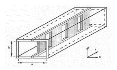
Waveguide Filters
Waveguides are hollow metal conduits with a circular or rectangular section. They are used for applications where a strong quality factor a good power handling and very low loss are needed such as RADAR or Satcom ground station. Their main disadvantage is that they are very bulky and often expensive.
Waveguide filters use mechanical elements such as metal inserts, iris, etc. to create, shift or couple resonant modes in order to create a filter function.
Cavity Filter
One way to create a resonance in a volume is to create a cavity. It is a geometrical hollow shape that will perturbate the signal propagation in a controlled manner, at a given frequency creating a resonant element. By cascading several cavities, we can then create a filter function. In order to get the precisely needed function beside the manufacturing tolerances, tuning screws are often used to adjust the frequencies and the coupling between the resonant elements.
Coaxial Cavity Filter
Coaxial cavity filters are made of an inner and an outer conductor separated by a dielectric material (such as air). The inner conductor length of a resonnator is λ/4. Depending on the desired function, these cavities can be arranged in several ways in order to set the desired resonances between the propagation modes.
Dielectric Resonator Filter
A dielectric resonator uses a piece of dielectric material (such as ceramics) with very high permittivity shaped usually as a puck. It functions as a traditional cavity resonator but the microwaves are reflected by the drastic permittivity change between the air and the dielectric puck. Dielectric resonators offer a strong reduction of cost and weight compared to metal cavities and waveguide filters. This technology becomes more and more interesting as new materials allow the dielectric resonator unloaded Q to be nearly as good as metal cavity ones.
Slabline (combline, interdigited) Filter
Slabline filters are filters that use side by side metallic rods. They are used to design pass band and band stop filters with a high unloaded Q factor. The frequencies are set when defining the rods length, and then the bandwidth is set by defining the spacing (therefore the coupling) between each rod.
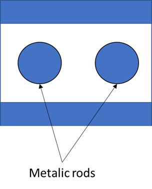
This technology can be use with two topologies:
- Interdigital filters:
An interdigital filter can be used to design band pass filter with a standard bandwidth. Side to side λ/4 resonators are coupled together. These resonators are alternatively terminated with an open or short circuit. This topology can also be used when designing a planar filter. The λ/4 rods are then replaced with λ/4 lines.
- Combline Filter:
This filter topology is very similar to interdigital. The main difference is that all the resonators are terminated by a short circuit on the same side. This topology can also be used with planar filters.
Technologies et applications : Planar
Type of dielectric substrate
A dielectric substrate is a non-conductive material used to manufacture printed circuit boards (PCB). The main characteristics of a substrate are:
Its permittivity ε’ also called dielectric constant (K). It translates the material capacity to store electrons in an electric field. The size of a rf printed circuit board will be reduced when the permittivity of the substrate is high.
Its dielectric loss ε’’, quantifies the amount of power loss inside the substrate. In general, the higher the permittivity is, the higher the dielectric loss is as well.
The thermal conductivity (W/mK), quantifies the ease for the material to transfer heat. This parameter is important because insertion loss inside a RF filter produces heat when the input power is high. If the losses are too strong (or the input power to high), and if the thermal conductivity is not good enough it can lead to an overheat of the circuit and potential physical degradation.
There is a large variety of substrate to choose from, when designing a planar filter.
- PTFE/Teflon
Laminated PTFE, is a type of flexible plastic, which is quite temperature stable. It offers good electrical and mechanical performances and is affordable.
It can also be charged with ceramics particles in order to enhance its permittivity or its thermal conductivity.
- Ceramic
Ceramics are dense and hard materials with high thermal capabilities and often a quite high permeability. The most used ceramics are Alumina (Al₂O₃) and Aluminum nitride (AlN). Manufacturing PCB out of ceramics requires costly means of production (laser cutting, silkscreen printing, etc.).
Type of planar filters
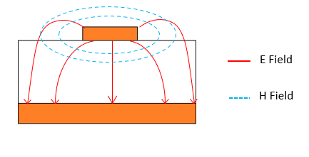
- Microstrip
Microstrip technology is a type of circuit board design used in electronic devices. It involves placing a thin layer of conductive material, such as copper, on a dielectric substrate. This layer of conductive material is used to create the electrical pathways or “traces” that form the circuit.
In microstrip technology, the conductive layer is typically placed on one side of the substrate, with a ground plane on the other side. The circuit traces are created by etching away portions of the conductive layer, leaving behind a pattern of conductive pathways.
One advantage of microstrip technology is that it allows for the creation of compact and lightweight circuits. It is commonly used in microwave and RF applications, because the thin conductive layer and dielectric substrate provide good electrical performance at high frequencies.
However, microstrip circuits can be susceptible to electromagnetic interference (EMI) and signal loss, particularly at higher frequencies. To minimize these effects, designers may use shielding techniques and carefully control the layout and placement of circuit elements.
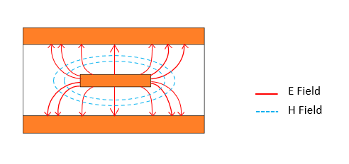
- Stripline
Stripline is a type of circuit board design used in electronic devices that is similar to microstrip technology but with some differences in the layering and construction of the circuit.
In a stripline design, the conductive layer is sandwiched between two layers of dielectric material, with ground planes on both sides. This creates a waveguide-like structure for the electrical signals, which travel along the center conductor between the two ground planes.
It offers several advantages over microstrip, including improved isolation from external electromagnetic interference. However, it is more complex and expensive to manufacture than microstrip technology.
Stripline technology is commonly used in high-frequency applications, where signal quality and noise reduction are critical. It is also used in applications where circuit density is not a primary concern, such as in some military and aerospace applications.
- Suspended substrate
Suspended substrate is a similar technology to stripline and microwave. The main differences is that that both side of the substrate can be used to transport signal as there is no ground plane. This allows to create well defined series capacitor by coupling the top and bottom layer traces. The ground plane is created by carving a cavity inside the top and bottom metal cases.
- Lumped elements
A lumped element Rf filter is constructed using discrete components (such as capacitors and inductors) rather than ones distributed throughout the circuit like in a transmission line. It is often used in “low” frequency application (<1GHz) where fully planar technologies are lossy and bulky. However, it can be used for higher frequency applications by employing SMD capacitors and inductors but it tends to show a low Q factor as the frequency goes up.
Type of topologies for planar filters
- Coupled lines
A planar coupled lines filter is a type of radio frequency (RF) filter that is designed using coupled transmission lines on a planar substrate. The coupled lines are typically made of parallel metal traces that run close to each other on the substrate, with a small gap between them.
A planar coupled lines filter uses the interaction between the electric fields of the coupled lines to selectively attenuate certain frequencies while allowing others to pass through. By adjusting the physical parameters of the coupled lines, such as their length, width, and separation distance, the filter is designed to have specific frequency response characteristics.
They offer several advantages over other types of RF filters, including their small size, low cost, and compatibility with integrated circuit fabrication processes.
It is mainly used to create bandstop or passband filter and can used a large array of coupled line technologies such as Hairpin, Edge-coupled, Combline, Interdigital, etc.
- Stepped
The basic principle of operation of a planar stepped line filter is that it uses the change in impedance along the length of the line to selectively attenuate certain frequencies while allowing others to pass through. By adjusting the physical parameters of the stepped lines, such as the length of each section, the width of each section, and the spacing between sections, the filter can be designed to have specific frequency response characteristics. It can be used to design lowpass and band pass filters.
- Stubs
Stubs are short or open-circuited at specific points to create a resonant structure that can selectively attenuate certain frequencies while allowing others to pass through.
The basic principle of operation of a planar stub filter is that it uses the reflections and interference created by the stubs to selectively filter out unwanted frequencies. By adjusting the physical parameters of the stubs, such as their length and position along the transmission line, the filter can be designed to have specific frequency response characteristics. It can be used to design all kinds of filters (Lowpass, Highpass, Bandpass, and Bandstop), depending on the configuration.
Technologies and applications : Other technologies
Substrate Integrated Waveguide (SIW)
Mechanical filters give very good electrical performances but with a high volume, high weight and high cost. On the contrary, planar solutions are low cost and show great compacity, but with more limited specification.
In order to combine the best of both worlds (in theory), the Substrate Integrated Waveguide (SIW) was invented. It incorporates a waveguide within a dielectric substrate. A row of metalized vias is used on both sides to make the side of the waveguide. This technology offers good Q factor compared to planar solutions and a reduction in cost compared to waveguide, however it is limited in terms of handling power.
Low Temperature Co-Fired Ceramics (LTCC)
LTCC stands for Low Temperature Co-Fired Ceramic. It is a type of ceramic material used in the manufacture of electronic components such as capacitors, inductors, filters, and resonators. LTCC is characterized by its ability to be co-fired with multiple layers of conductive and non-conductive materials, allowing for the creation of complex electronic circuits in a single package.
The low-temperature firing process used in LTCC manufacturing involves heating the ceramic material to a relatively low temperature, typically between 850°C and 900°C, which helps to reduce the cost of production and improve the performance of the electronic components.
But because of its design complexity and cost of implementation it is not suitable for low quantity applications, as the initial design cost is high.
Miscellaneous filter types
Multiplexer
In telecommunication systems in a spatial, military of civilian environments, it is sometimes needed to divide or recombine different frequency ranges. As an example, in satellites applications, to allow the sender to just send one canal and not all of them.
Demultiplexing is dividing the input signal into a number n of canals, with a fixed bandwidth defined by the application. Multiplexing, on the other hand, is taking n canals and recombining them on the same output. In order to achieve such functions, several parallel filters are used. All filter topologies and technologies seen above can be used for this purpose, depending on the behavior needed.
It differs from a Power Combiner as it can combine two clearly separated bandwidth.
Bias Tee
Bias tee are RF passive components used in applications where a DC current needs to be injected without perturbations on the rf signal. This kind of devices, shaped as a T (hence the name), has 3 Ports: RF signal, DC current and RF signal + DC current
They are used to supply power to amplifiers, active antennas or any other devices that need DC current to run.
DC block
DC-Blocks are two ports passive components used to suppress any DC coming in while leaving untouched any RF signal. They are usually used to protect the transmission chain.